
25 2 月
The Race Is Already On
Few industries have attracted the level of geopolitical attention, capital commitment, and policy urgency that semiconductors have over the past five years. What was once a specialised corner of the electronics sector is now explicitly framed, by Washington, Brussels, Tokyo, and New Delhi alike, as strategic infrastructure. The reason is straightforward: chips are the enabling layer beneath virtually everything that defines modern economic competitiveness.
The numbers reflect this urgency. Global semiconductor revenues reached approximately USD 627 billion in 2024 and are forecast by the World Semiconductor Trade Statistics (WSTS) to approach USD 975 billion by 2026, a compounded growth rate that few other industries can match. AI-related chips alone saw a 39.9% year-on-year increase in sales, reaching USD 301.9 billion in 2025. Memory chips followed closely with 34.8% growth. These are not incremental market expansions; they are structural shifts driven by the convergence of artificial intelligence, 5G infrastructure build-out, electric vehicle proliferation, and the broad digitisation of industrial systems.
The competitive landscape is moving just as fast. TSMC began volume production of its 2nm (N2) process node in Q4 2025. ASML unveiled an EUV light source advance expected to yield 50% more chips per system by 2030. The US CHIPS and Science Act, EU Chips Act, and India’s Semicon India programme have collectively committed well over USD 100 billion in public incentives to attract fabrication capacity. For late entrants, watching from the sidelines is not a neutral position. The question for Bangladesh is not whether to engage, but where and how, given what it can credibly build in the near term.
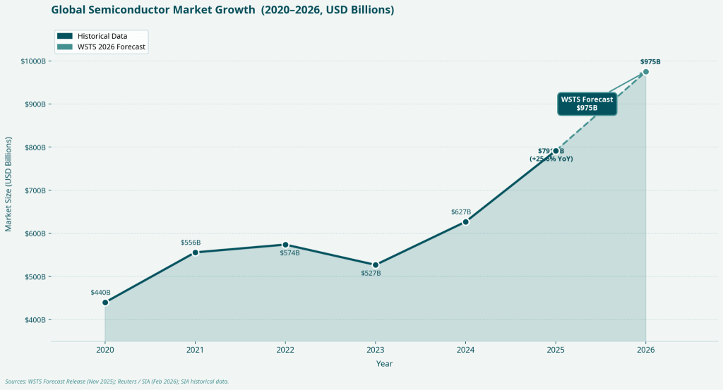
Figure 1: Global semiconductor market revenue forecast to USD 975 billion by 2026. Source: WSTS Forecast Release, 2025.
What Makes Semiconductors a Strategic Asset
A semiconductor chip is, at its core, a silicon wafer patterned with billions of microscopic transistors that act as controlled switches — capable of performing calculations, storing data, and routing signals at extraordinary speed. The power of chips lies in their compounding: Moore’s Law observed that transistor counts double roughly every two years, enabling leaps in performance per watt while driving down the cost of computing over time. Even as the physics of miniaturisation reaches its limits at the leading edge, advanced packaging techniques and specialised accelerators continue to extend that trajectory.
But the strategic importance of semiconductors goes well beyond engineering elegance. Consider what market leadership in this industry actually means. TSMC’s foundry business, accounting for roughly 60% of global contract chip manufacturing, gives Taiwan asymmetric leverage in global supply chains. South Korea’s dominance in DRAM and NAND memory through Samsung and SK Hynix means that virtually every data centre, smartphone, and server depends on Korean production decisions. The US, through firms like Nvidia, Qualcomm, and AMD, commands the design and intellectual property layer that defines what the next generation of chips can do. ASML, a Dutch company, holds a near-monopoly on the extreme ultraviolet lithography equipment without which the most advanced chips cannot be manufactured at all.
These are not merely market positions — they are structural chokepoints that confer negotiating leverage, export revenue, and long-term innovation optionality. The countries that have built credibility in semiconductors have done so by choosing the right stage of the value chain to master, scaling it with discipline, and integrating deeply into the networks of global OEMs and system integrators who cannot afford their supply chains to fail. That template is available to new entrants, but only in the segments where access to advanced equipment and established ecosystems is not a prerequisite.
Navigating the Global Value Chain
How the chain is structured
The semiconductor value chain is best understood as four distinct stages, each with its own economics, bottlenecks, and required capabilities. Design is where architects and engineers translate product requirements into detailed circuit layouts, verify them against functional specifications, and produce the intellectual property that determines what a chip can do. Fabrication is where those designs are physically realised on silicon wafers through capital-intensive, precision manufacturing processes. Assembly and Packaging follows fabrication, cutting wafers into individual dies and encasing them in forms suitable for integration into devices. Finally, Testing — often handled by specialised Outsourced Semiconductor Assembly and Test (OSAT) providers — validates the performance and reliability of each component at scale before it enters the supply chain.
Each stage has a fundamentally different entry calculus. Fabrication at the leading edge requires tens of billions of dollars in capital expenditure, access to ASML’s EUV lithography systems (which cost upwards of USD 350 million each), and a supply chain ecosystem that takes decades to build. OSAT and design services, by contrast, are human capital and process-intensive, scalable incrementally, and actively sought by global chipmakers looking to reduce costs and diversify their supplier base.
Demand across node tiers — where access is possible
Not all chip demand is for cutting-edge nodes. While the AI boom drives headlines around 2–5nm chips, a substantial share of the global semiconductor market, covering microcontrollers, power management ICs, automotive subsystems, appliance controllers, and industrial sensors, continues to be served by mature-node chips at 15nm and above, often at 28nm and beyond. These segments are not shrinking; they are growing in absolute terms as electrification and automation drive demand across sectors that have nothing to do with AI.
This distinction matters for market entry. Sub-5nm fabrication requires EUV lithography and dense supplier ecosystems confined to Taiwan, South Korea, and a handful of US fabs. Sub-15nm advanced nodes are similarly concentrated. But the 15nm-and-above tier sustains a diverse global supplier base, is actively being expanded (including by China, which is investing heavily in mature-node capacity), and contains the design verification, testing, and OSAT services that new entrants can enter without controlling a fab.
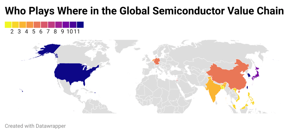
| 1 | 2–3 | 4–6 | 7–9 | 10–11 | 12 |
| Entry Stage — Design Services Nascent (15+ nm) | Mature Node Participation — Assembly and Test Focus (15+ nm) | Mature Node Dominant with Limited Advanced Presence (15+ nm) | Advanced Mainstream to Mature — Aspirational or Emerging at Leading Edge (7-14 nm) | Advanced to Leading Edge — Near Full Spectrum (Emerging in 2–3nm) | Full Spectrum — Active Across All Tiers (Leads 2–3nm) |
Figure 2: Geographic distribution of semiconductor fabrication capability by node tier. Red: 2nm nodes (Taiwan, US, Korea); Yellow: sub-15nm advanced nodes; Green: 15nm+ mature nodes with broader global participation. Source: Synthesised from OECD data.
The map above illustrates a clear pattern: the most advanced nodes are tightly concentrated among a handful of economies with decades of ecosystem investment behind them. The 15nm+ mature tier, by contrast, shows broader geographic participation — and it is here, alongside the design services and test engineering layers that cut across all node tiers, that the structural opening exists for new market
entrants. The semiconductor landscape can be understood as a progression of capability across node tiers.
At the earliest stage sit countries with nascent design services exposure, participating primarily in the 15nm-and-above mature-node ecosystem without fabrication depth. The next layer consists of economies focused on assembly and test within the mature-node tier, building competence through OSAT and backend integration rather than wafer production.
Further up are countries that dominate mature-node fabrication while maintaining only limited presence in advanced nodes. Beyond them are those operating across both mature and advanced mainstream nodes (7–14nm), with aspirational or emerging exposure to leading-edge technologies.
Near the top are semiconductor powers spanning advanced to leading-edge manufacturing, including early movement into 2–3nm processes. At the apex sit the few economies with full-spectrum capability, active across design, fabrication, packaging, and testing — and leading global production at the 2–3nm frontier.
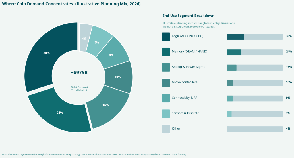
Figure 3: Semiconductor end-use category shares. Memory and Logic dominate, but significant demand flows to automotive, industrial, and consumer segments served by mature nodes. Source: WSTS category data.
Bangladesh’s Window: Realistic Entry, Credible Trajectory
Early signals worth building on
Bangladesh’s semiconductor ambitions are not starting from scratch. In 2022, the country earned USD 6 million in semiconductor design services exports — a modest number, but a real one. By 2024, that figure had risen to USD 8 million, with nearly 700 chip designers engaged across the industry. The Bangladesh Semiconductor Industry Association (BSIA) has set an export target of USD 1 billion by 2030, and the government has established a national taskforce under BIDA to develop the sector, with a focus on chip design, testing, and assembly incentives. A collaboration between BSIA and the Hubei Semiconductor Industry Association (HSIA) has created early channels for technology exchange and workforce development.
None of this amounts to a semiconductor industry yet. But it represents the kind of early ecosystem formation, policy intent, skills base, and institutional connectivity that, if properly structured, can be compounded into a credible market position over the next five to seven years.
The cost advantage is real, but not sufficient on its own
Operating costs in Dhaka run 16–20% below Bangalore and approximately 30% below Cebu — two of the most active semiconductor services hubs in Asia. For global chipmakers and fabless design houses under pressure to reduce engineering costs without compromising quality, that gap is meaningful. India’s design ecosystem has demonstrated that cost-competitive, quality-assured engineering talent can absorb substantial outsourced workloads from US, European, and Japanese firms.
The challenge is that cost alone does not win contracts in semiconductors. What wins contracts is demonstrated execution quality, the institutional infrastructure (testing labs, IP protection frameworks, export clearance systems) that large clients require before committing work, and the talent pipeline depth that allows engagements to scale without breaking. Bangladesh’s gap is not primarily in cost or intent — it is in building the credibility signals that global buyers need to see.
Where to focus: a phased view
Based on where global demand is growing and where Bangladesh’s current capabilities sit, the most productive near-term concentration is in the 15nm+ mature node tier, specifically in design verification, design for test (DFT), test engineering services, and the OSAT entry pathway. The table below maps node tiers to their current global supply landscape and Bangladesh’s most credible entry points.
Table 1: Node tiers, global supply landscape, and Bangladesh entry points
| Node Band | Typical Products | Current Leaders | Bangladesh Entry Point |
| 2–5nm (Leading Edge) | AI accelerators, flagship mobile SoCs | TSMC, Samsung, US/Korea ecosystems (EUV-intensive) | Design verification support, physical design services, EDA tool integration |
| 7–14nm (Advanced) | High-end consumer chips, networking, data centre | Taiwan, South Korea, select US/EU supply chain | DFT (design for test), validation engineering, firmware-test integration |
| 15nm+ / ≥28nm (Mature Node) | PMICs, MCUs, appliances, industrial controls, automotive subsystems | Diverse global base; China rapidly expanding capacity | OSAT entry, test engineering, reliability labs, EMS-to-OSAT bridge — primary near-term focus |
Source: TSMC Technology Node disclosures; Mordor Intelligence; WSTS.
The 2–5nm design verification row is worth noting: Bangladesh need not wait until it can fabricate at the leading edge to participate in leading-edge chip economics. Design support services for advanced-node projects — verifying layouts, validating timing, running test simulations — are increasingly outsourced by fabless design houses. This is a talent play, not a capital play, and it is one Bangladesh can begin building toward immediately alongside the more accessible mature-node OSAT pathway.
A Perspective Worth Holding
Our reading of the data and the competitive landscape leads us to a view that is neither pessimistic nor uncritically optimistic. Bangladesh is unlikely to be competing with TSMC or Samsung for leading-edge fabrication contracts within any planning horizon that is relevant today. That is simply not the opening that the market structure provides.
What the market does provide — and what the 2026 demand trajectory reinforces — is a growing need for reliable, cost-competitive execution in the design services, test engineering, and OSAT segments that sit adjacent to the capital-intensive core. These are the segments where Vietnam, Malaysia, and parts of India have built durable export positions, and where the barriers to entry are defined by quality systems and talent rather than by billions in equipment spend.
The 2030 target of USD 1 billion in semiconductor exports is ambitious relative to the current base, but not structurally implausible if the policy backbone is built correctly, the talent pipeline is developed with the right curriculum and industry linkages, and early partnerships with global firms create the reference cases that subsequent clients require. The window that 2026 demand dynamics open is real. Whether Bangladesh steps through it in a way that compounds into a durable industry position depends on choices that need to start now.
References
1. World Semiconductor Trade Statistics (WSTS). Global Semiconductor Market Approaches $1T in 2026. https://www.wsts.org/76/Global-Semiconductor-Market-Approaches-1T-in-2026
2. Reuters. Global chip sales expected to hit $1 trillion this year, industry group says. February 2026. https://www.reuters.com/business/global-chip-sales-expected-hit-1-trillion-this-year-industry-group-says-2026-02-06/
3. TSMC. N2 Technology Node. https://www.tsmc.com/english/dedicatedFoundry/technology/logic/l_2nm
4. ASML. EUV Lithography Systems. https://www.asml.com/products/euv-lithography-systems
5. Reuters. ASML unveils EUV light source advance. February 2026. https://www.reuters.com/world/china/asml-unveils-euv-light-source-advance-that-could-yield-50-more-chips-by-2030-2026-02-23/
6. WSTS Forecast Release, November 2025. https://www.wsts.org/esraCMS/extension/media/f/WST/7310/WSTS_FC-Release-2025_11.pdf
7. The Daily Star. Taskforce led by BIDA formed for semiconductor sector. https://www.thedailystar.net/business/news/taskforce-led-bida-formed-semiconductor-sector-3789596
8. TBS News. Bangladesh eyes $1 billion semiconductor exports by 2030. https://www.tbsnews.net/tech/bangladesh-eyes-1-billion-semiconductor-exports-2030-991531
9. Bits & Chips. China’s chip industry uses 35% domestically sourced equipment. https://bits-chips.com/article/chinas-chip-industry-uses-35-percent-domestically-sourced-equipment/
10. BSS News. BSIA–HSIA partnership. https://www.bssnews.net/business/305057